ELECTRICAL DIAGRAMS AND SCHEMATICS
To read and understand an electronic diagram or electronic schematic, the basic symbols and conventions must be understood.
Menu
1 Electronic Diagrams, Prints, and Schematic
1.1 Introduction
1.2 Electronic Schematic Drawing Symbology
1.3 Examples of Electronic Schematic Diagrams
1.4 Reading Electronic Prints, Diagrams and Schematics
1.5 Block Drawing Symbology
1.6 Examples of Block Diagrams
Introduction
Electronic prints fall into two basic categories, electronic schematics and block diagrams.
Electronic schematics represent the most detailed category of electronic drawings. They depict every component in a circuit, the component's technical information (such as its ratings), and how each component is wired into the circuit. Block diagrams are the simplest type of drawing. As the name implies, block diagrams represent any part, component, or system as a simple geometric shape, with each block capable of representing a single component (such as a relay) or an entire system. The intended use of the drawing dictates the level of detail provided by each block. This chapter will review the basic symbols and conventions used in both types of drawings.
Electronic Schematic Drawing Symbology
Of all the different types of electronic drawings, electronic schematics provide the most detail and information about a circuit. Each electronic component in a given circuit will be depicted and in most cases its rating or other applicable component information will be provided. This type of drawing provides the level of information needed to troubleshoot electronic circuits.
Electronic schematics are the most difficult type of drawing to read, because they require a very high level of knowledge as to how each of the electronic components affects, or is affected by, an electrical current. This chapter reviews only the symbols commonly used in depicting the many components in electronic systems. Once mastered, this knowledge should enable the reader to obtain a functional understanding of most electronic prints and schematics.
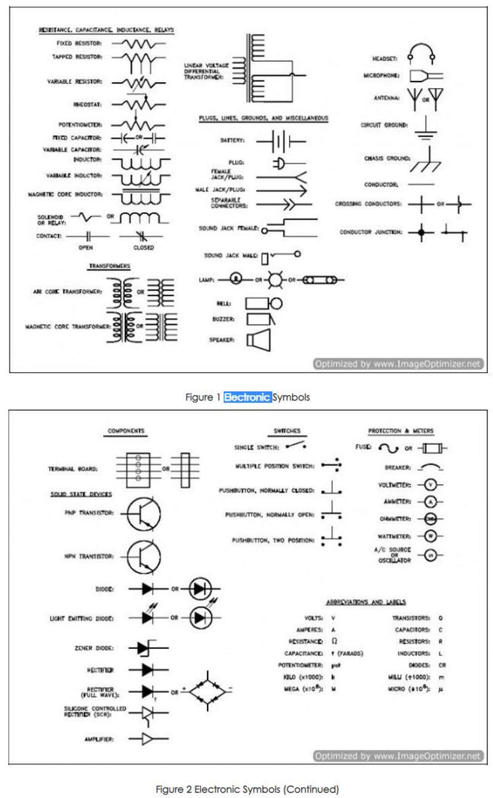
Figure 1 and Figure 2 illustrate the most common electronic symbols used on electronic schematics.
Examples of Electronic Schematic Diagrams
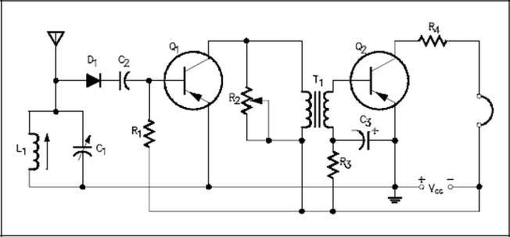
Electronic schematics use symbols for each component found in an electrical circuit, no matter how small. The schematics do not show placement or scale, merely function and flow. From this, the actual workings of a piece of electronic equipment can be determined. Figure 3 is an example of an electronic schematic diagram.
Figure 3 Example of an Electronic Schematic Diagram
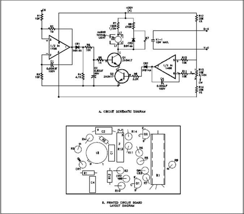
A second type of electronic schematic diagram, the pictorial layout diagram, is actually not so much an electronic schematic as a pictorial of how the electronic circuit actually looks. These drawings show the actual layout of the components on the circuit board. This provides a two-dimensional drawing, usually looking down from the top, detailing the components in their location. Shown in Figure 4 is the schematic for a circuit and the same circuit drawn in pictorial or layout format for comparison. Normally the pictorial layout would be accompanied by a parts list.
Figure 4 Comparison of an Electronic Schematic Diagram and its Pictorial Layout Diagram
Figure 4 Comparison of an Electronic Schematic Diagram and its Pictorial Layout Diagram

Reading Electronic Prints, Diagrams and Schematics
To properly read prints and schematics, the reader must identify the condition of the components shown and also follow the events that occur as the circuit functions. As with electrical systems, the relays and contacts shown are always in the de-energized condition. Modern electronic systems usually contain few, if any, relays or contacts, so these will normally play a minor role.
Electronic schematics are more difficult to read than electrical schematics, especially when solid state devices are used. Knowledge of the workings of these devices is necessary to determine current flow. In this section, only the basics will be covered to assist in reading skills.
The first observation in dealing with a detailed electronic schematic is the source and polarity of power. Generally, power will be shown one of two ways, either as an input transformer, or as a numerical value. When power is supplied by a transformer, polarity marks will aid in determining current flow. In this convention, dots on the primary and secondary indicate current flow into the primary and out of the secondary at a given instant of time. In Figure 5, the current is into the top of the primary and out of the bottom of the secondary.
Figure 5 Transformer Polarity Markings
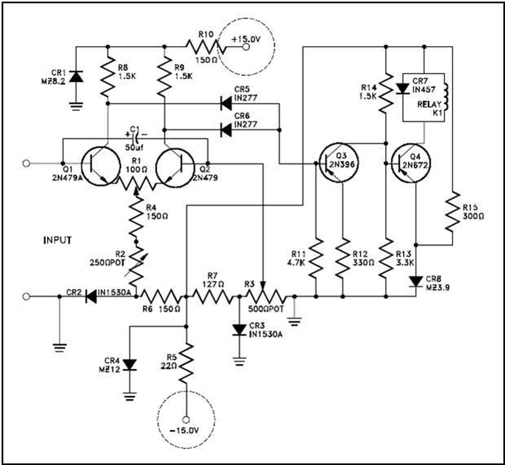
Generally, the electrical power source is indicated at the point where it enters a particular schematic. These values are stated numerically with polarity assigned (+15 volts, -15 volts). These markings are usually at the top and bottom of schematics, but not always. In the example shown in Figure 6, power is shown at both the top and bottom in a circuit using two power sources. Unless specified as an Alternating Current (AC) power source, the voltages can normally be assumed to be Direct Current (DC).
Figure 6 Schematic Showing Power Supply Connections
In any circuit, a ground must be established to create a complete current path. Ground is usually depicted by the use of the ground symbol that was shown previously. The direction of current flow can be determined by observing the polarity of the power supplies. When polarities are shown, current flow can be established and ground may not always be shown.
With the power sources located and the ground point established, operation of the devices can be determined.
The most common semiconductor devices are the transistor and the diode. They are made from materials like silicone and germanium, and have electrical properties intermediate between conductors and insulators. The semiconductor will be one of two varieties, the PNP or NPN.
The designation indicates the direction the electrons move through the device. The direction of the arrow indicates type, as shown in Figure 2. There are, however, many different ways to install a transistor to achieve different operational characteristics. These are too numerous to cover here, so only the most common and basic configuration (the common emitter) will be shown.
Even though transistors contain multiple junctions of p- or n-type material, current flow is generally in the same direction. Using conventional current flow (i.e. from + to -), current will travel through the transistor from most positive to least positive and in the direction of the arrow on the emitter. In Figure 7, the transistor has a positive power supply with ground on the emitter. If the input is also positive, the transistor will conduct.
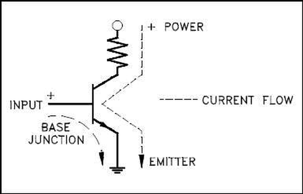
Figure 7 NPN Transistor-Conducting
If the input goes negative, as in Figure 8, the conduction of the device stops because the input, or in this case the base junction, controls the transistor condition. Notice that when current flows, it does so in the direction of the arrow.
If the input goes negative, as in Figure 8, the conduction of the device stops because the input, or in this case the base junction, controls the transistor condition. Notice that when current flows, it does so in the direction of the arrow.
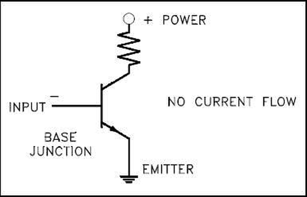
Figure 8 NPN Transistor-Nonconducting
Figure 9 uses a PNP transistor. The same rules apply as above except that this time polarities of power must change to allow current flow.
Figure 9 uses a PNP transistor. The same rules apply as above except that this time polarities of power must change to allow current flow.

Figure 9 NPN Transistor
The same rules that apply to transistors hold true with diodes. However, diodes are simpler than transistors because they have only one junction and conduct in only one direction, as indicated in Figure 10. The diode symbol, like the transistor symbol, shows the direction of conduction by the direction of the arrow, which is from positive to negative.
The same rules that apply to transistors hold true with diodes. However, diodes are simpler than transistors because they have only one junction and conduct in only one direction, as indicated in Figure 10. The diode symbol, like the transistor symbol, shows the direction of conduction by the direction of the arrow, which is from positive to negative.
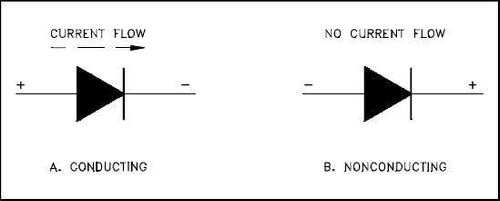
Figure 10 Diode
Although these simple rules will not allow you to read all electronic schematics, they will aid in understanding some of the basic concepts.
An item that may cause confusion when reading electronic prints or schematics is the markings used to show bistable operation. In most cases, bistables will be indicated by a box or circle, as shown in Figure 11 (A). The lines in or around these bistables not only mark them as bistables, but also indicate how they function.

Figure 11 Bistable Symbols
Figure 11 (B) shows the various conventions used to indicate bistable operation. Commonly, one circuit will interface with other circuits, which requires a method that allows the reader to follow one wire or signal path from the first drawing to the second. This may be done in many ways, but generally the line or conductor to be continued will end at a terminal board. This board will be labeled and numbered with the continuation drawing indicated (a separate drawing may exist for each line). With the next drawing in hand, only the terminal board that matches the previous number needs to be found to continue. In cases where terminal boards are not used, the conductor should end with a number (usually a single digit) and also the next drawing number. To assist in locating the continuation, coordinates are provided on some drawings that indicate the location of the continuation on the second drawing. The continuation point on the second drawing will also reference back to the first drawing and the coordinates of the continuation.
Block Drawing Symbology
Not all electronics prints are drawn to the level of detail depicting the individual resistors and capacitors, nor is this level of information always necessary. These simpler drawings are called block diagrams. Block diagrams provide a means of representing any type of electronic circuit or system in a simple graphic format. Block diagrams are designed to present flow or functional information about the circuit or system, not detailed component data. The symbols shown in Figure 12 are used in block diagrams.
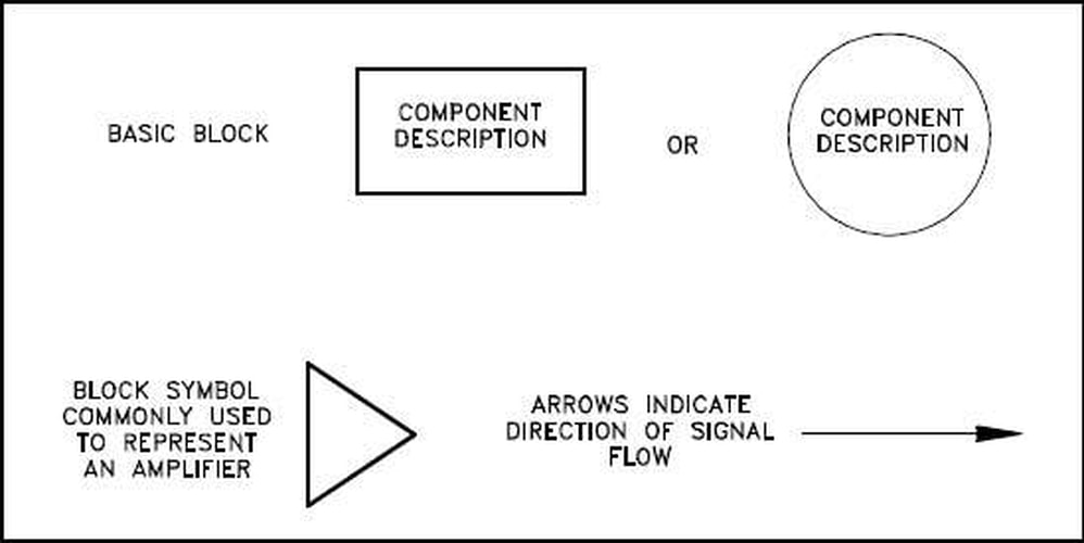
Figure 12 Example Blocks
When block diagrams are used, the basic blocks shown above (Figure 12) can be used for almost anything. Whatever the block represents will be written inside. Note that block diagrams are presented in this chapter with electronic schematics because block diagrams are commonly found with complex schematic diagrams to help present or summarize their flow or functional information. The use of block diagrams is not restricted to electronic circuits. Block diagrams are used extensively to show complex instrument channels and other complex systems when only the flowpath of the signal is important.
Examples of Block Diagrams
The block diagram is the most basic and easiest to understand of all the types of engineering prints. It consists of simple blocks that can represent as much, or as little, as desired. An example of a block diagram is shown in Figure 13.
This particular block diagram represents an instrumentation channel used to measure the neutron flux, indicate the measured flux, and generate output signals for use by other systems.
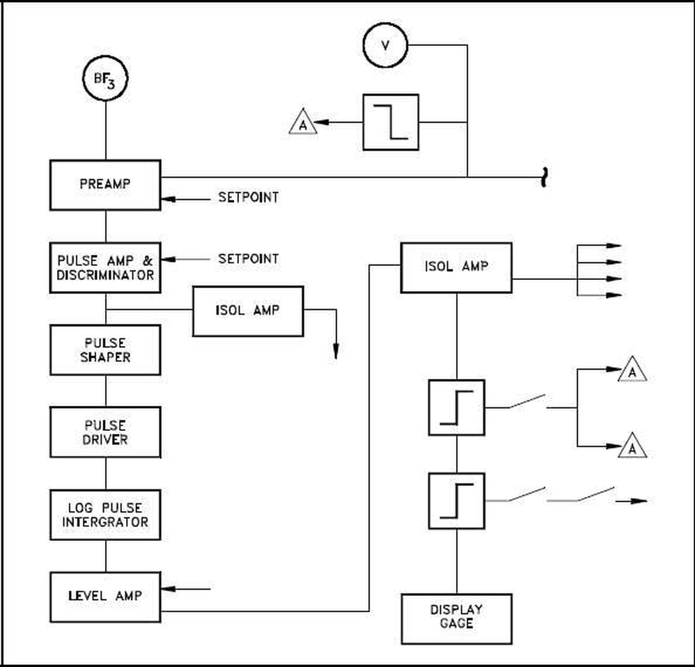
Figure 13 Example Block Diagram
Each block represents a stage in the development of a signal that is used to display on the meter at the bottom or to send to systems outside the bounds of the drawing. Notice that not all blocks are equal. Some represent multiple functions, while others represent only a simple stage or single bistable circuit in a larger component. The creator of the block diagram decides the content of each block based on the intended use of the drawing.
Each of the type of drawing reviewed in this and previous modules is not always distinct and separate. In many cases, two or more types of drawings will be combined into a single print. This allows the necessary information to be presented in a clear and concise format.
Figure 14 provides a sample illustration of how the various types of drawings can be combined. In this example, mechanical symbols are used to represent the process system and the valves controlled by the electrical circuit; electrical single line symbols are used to show the solenoid relays and contacts used in the system; and electronic block symbols are used for the controllers, summers, I/P converter, and bistables.
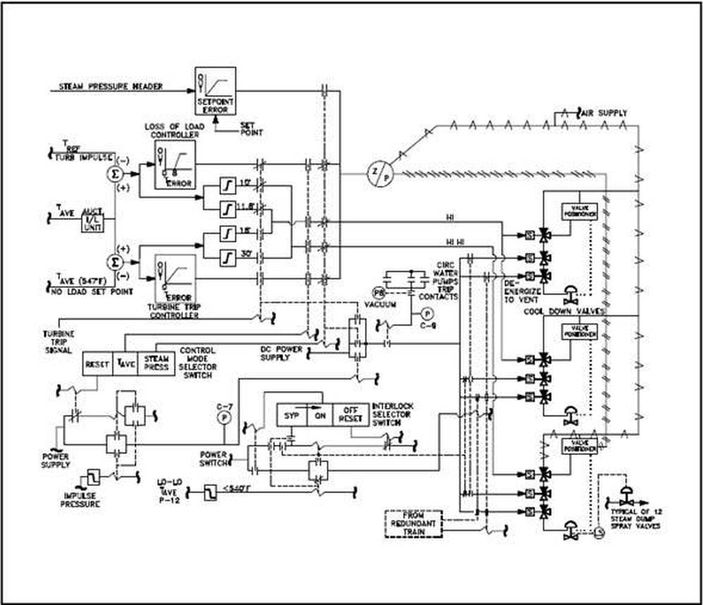
Figure 14 Example of a Combined Drawing, P & ID, Electrical Single Line, and Electronic Block Diagram
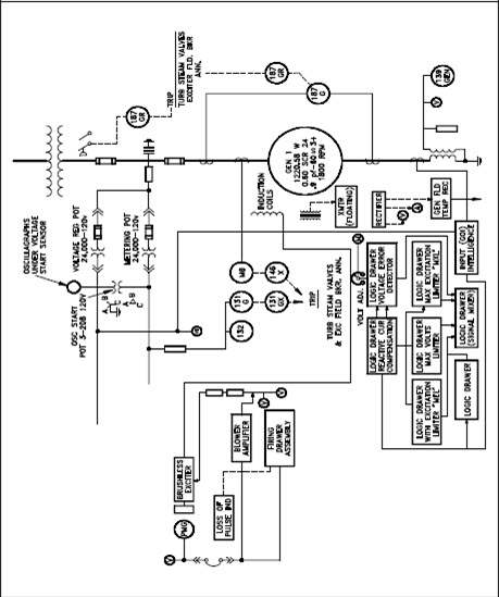
Figure 15 illustrates the use of an electronic block diagram combined with an electrical single line diagram. This drawing represents a portion of the generator protection circuitry of a power generating plant.
Figure 15 illustrates the use of an electronic block diagram combined with an electrical single line diagram. This drawing represents a portion of the generator protection circuitry of a power generating plant.
Figure 15 Example Combination Diagram of Electrical Single Line, and Block Diagram
